
Technical visual reference
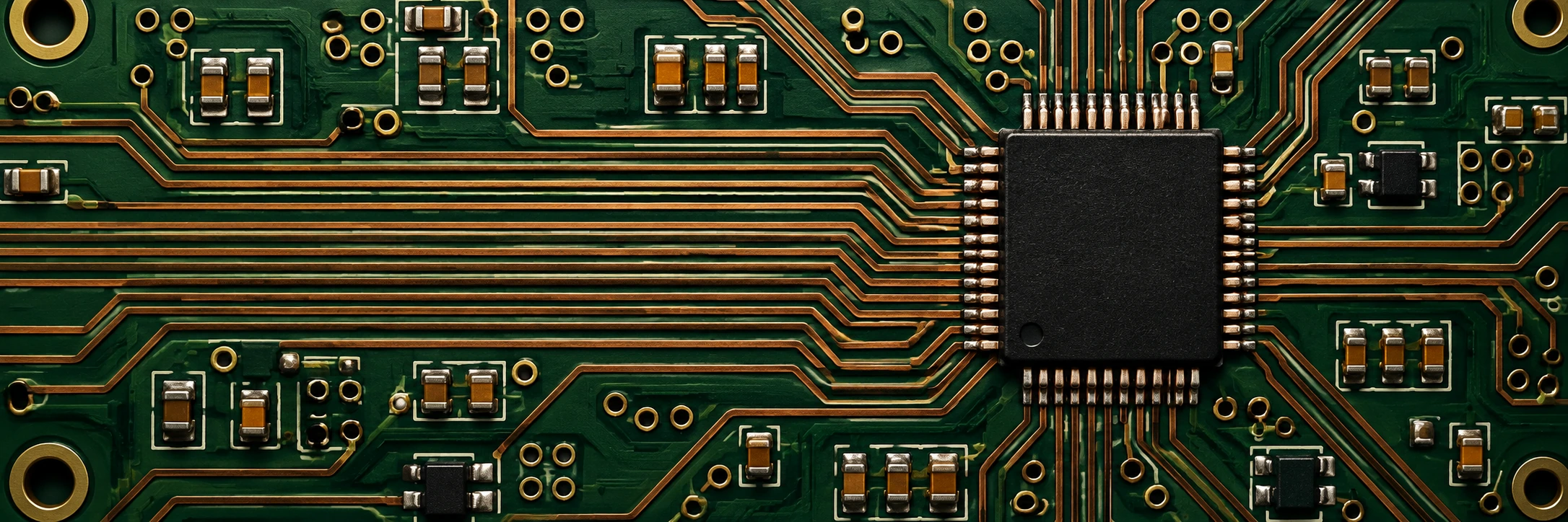
Printed Circuit Board translates the designed surface of electronics into an image language: routed lines, contact pads, repeated components and carefully reserved gaps. Its beauty comes from relationships and constraints, not simply from adding green to a futuristic picture.
A visual introduction
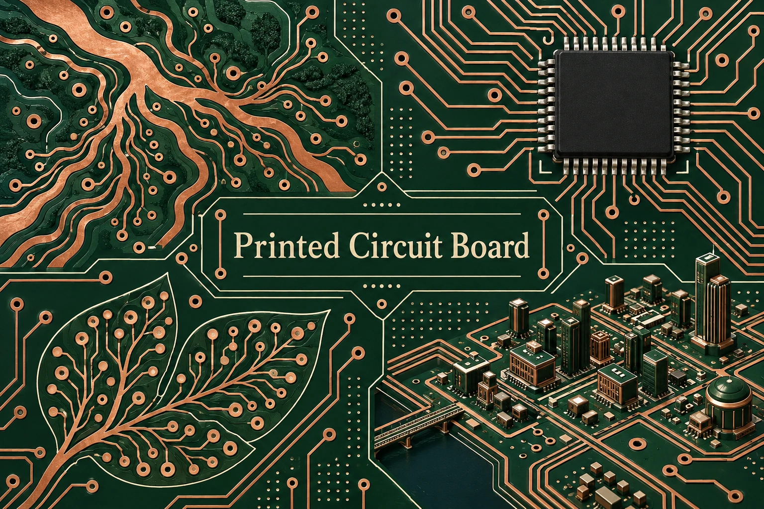
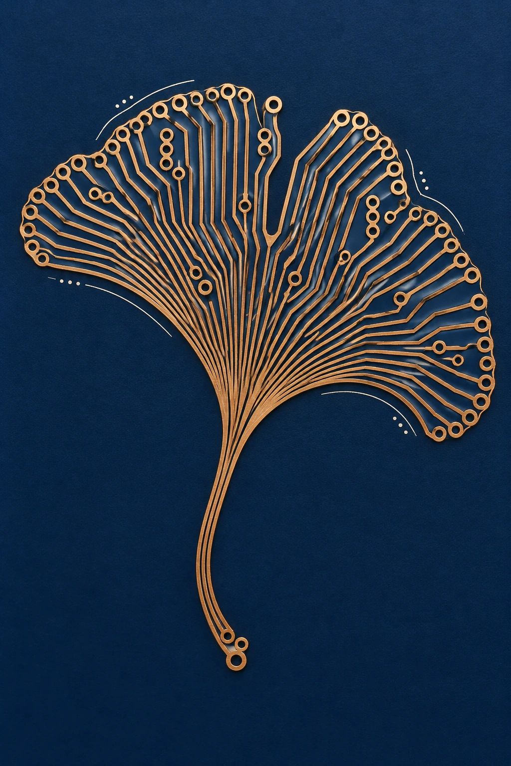
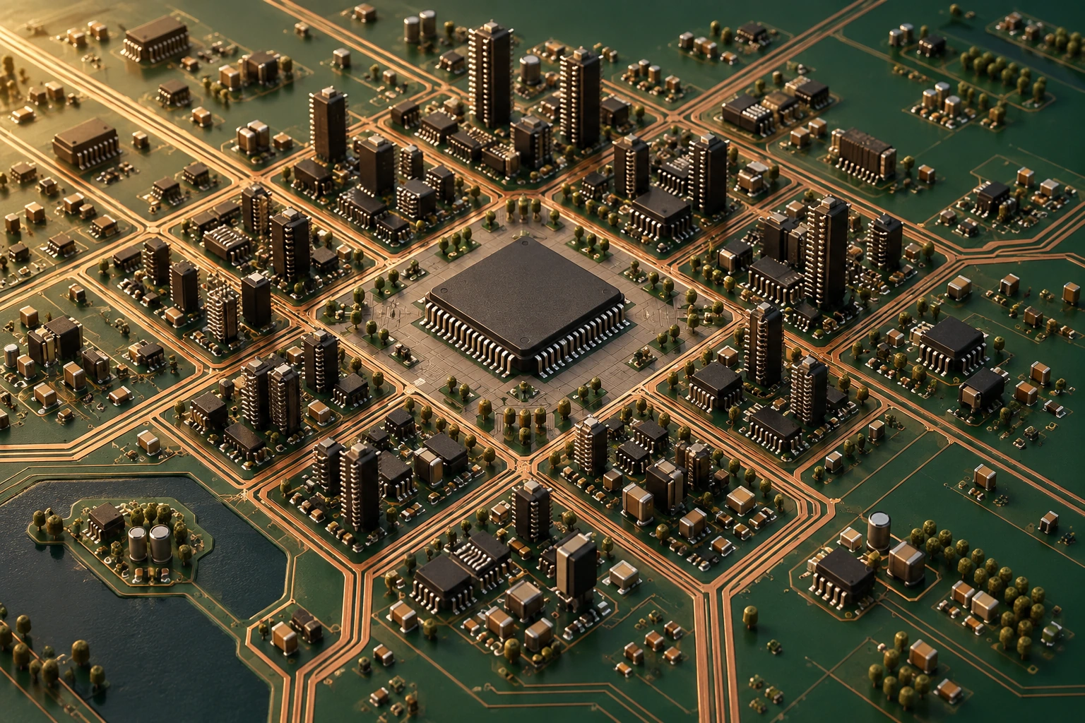
Five original AI-generated AOI interpretations: a dedicated banner, a centrally titled collage and three standalone studies. These images are not historical works or technical fabrication documents.
Select an image for a closer look. Use the thumbnails, arrow keys or a swipe to compare examples. Zoom in to inspect details, or share the image that inspires you.
Creative toolbox · take this style further
Choose an input and a destination. Search sends your words to the chosen site; Copy & open puts them on your clipboard to paste there.
Create with AI
Turn your chosen input into an image prompt or a new creative direction.
ChatGPT
Copy your input and paste it into a ChatGPT conversation or image request.
Copy & open ChatGPT (new tab)Claude · Anthropic
Develop an image prompt or explore the style in a new Claude conversation.
Copy & open Claude · Anthropic (new tab)Midjourney
Paste your input into the Imagine bar on the Create page.
Copy & open Midjourney (new tab)Adobe Firefly
Copy your input, open Firefly, and paste it into the prompt field.
Copy & open Adobe Firefly (new tab)Leonardo.Ai
Copy your input, open Leonardo, and paste it into the generation field.
Copy & open Leonardo.Ai (new tab)Image search
Find visual references. Short, concrete keywords usually work best.
Lexica
Search AI images and prompts using your selected input.
Search with this input Lexica (new tab)Pexels
Search the photo and video library. Short keywords often work best.
Search with this input Pexels (new tab)Pixabay
Search photos, illustrations and other images.
Search with this input Pixabay (new tab)Unsplash
Search photographs using the style name or your own keywords.
Search with this input Unsplash (new tab)Wikimedia Commons
Search photographs, artworks and historical images. Check each file for its source and reuse terms.
Search with this input Wikimedia Commons (new tab)Art & research
Explore artists, collections and the ideas behind a style.
Wikipedia
Search for background reading. A style may not have its own article.
Search with this input Wikipedia (new tab)WikiArt
Copy your input into WikiArt’s search to explore artists and artworks.
Copy & open WikiArt (new tab)Europeana
Paste your keywords into the search to explore European museum, library and archive collections.
Copy & open Europeana (new tab)Inspiration
Discover portfolios and visual ideas from creative communities.
Instagram hashtags
Search a hashtag made from your input: spaces and punctuation are removed. Instagram may require sign-in.
Search with this input Instagram hashtags (new tab)ArtStation
Paste your input into artwork search for concept art, environments, characters and visual development.
Copy & open ArtStation (new tab)Behance
Paste your input into project search for illustration, design and visual storytelling.
Copy & open Behance (new tab)A closer look
Parallel conductive-looking tracks, angular route changes, circular vias, rectangular pads, component arrays and fine silkscreen outlines layered over a flat soldermask-coloured field.
From an engineered object to an artistic vocabulary
A printed circuit board is an engineered support and interconnection structure for electronic components. In this AOI article, its name identifies a visual reference, not a historical art movement. The artistic attraction lies in an unusual combination: strict repetition at the scale of pins and pads, meandering routes at the scale of a board, and a few large components that organise the whole field. A close view can read like a map; an oblique view can suggest a miniature built environment.
The illustrations here borrow that grammar for a leaf, a city and a moth. These are imaginative transformations, not validated board layouts. A plausible-looking route does not establish electrical continuity, suitable spacing or a functioning device. Keeping this distinction visible allows the pictures to explore metaphor without pretending that decorative imagery is engineering documentation.
Read the layers before inventing the picture
PCB design documentation distinguishes copper layers from solder mask, silkscreen and other technical layers. Tracks carry connections; pads provide connection areas; vias connect between layers. These terms describe different jobs, even when all appear as attractive marks in a flat image. KiCad’s PCB Editor documentation is a useful primary reference for understanding the vocabulary and the relationship between layers, tracks and vias.
For an artistic study, translate these differences into clearly separated visual behaviours: continuous tracks as line, pads as repeated nodes, component bodies as larger masses and silkscreen as a fine overlay. A green ground is familiar, but blue, dark purple or black can preserve the same structure. Colour alone does not define the style. Nor should every track be depicted as bright exposed copper: that is a deliberate artistic emphasis in several AOI studies rather than a universal description of manufactured boards.
Composition: route the viewer’s attention
Start with one large anchor, such as a rectangular chip or the central body of an insect. Arrange smaller units around it, then let parallel tracks connect the areas visually. A consistent track width and a limited set of bend angles help the surface feel designed. The familiar forty-five-degree turn is a useful graphic convention here, not a claim that every real board must use it. Leave controlled gaps between line groups so their direction remains legible.
Density should vary. A crowded central junction can be balanced by an open perimeter; a narrow bundle of tracks can spread into a broad fan. Repeated pads establish rhythm, while one change of scale creates a focal point. Resist the temptation to fill every available space with another component. Empty board areas are valuable compositional pauses. In an imaginary circuit, they also make it easier for viewers to understand which forms are meant to belong together.
Material, lighting and useful transformations
A convincing material study separates matte component bodies, smooth board coating and reflective metallic details. Use raking light to reveal shallow relief without turning every line into a glowing tube. Warm copper against a deep cool field creates separation; restrained cream outlines can clarify shapes. For a flat editorial illustration, simplify the lighting and let spacing carry the depth. For a miniature city, introduce a low oblique viewpoint so pins, packages and traces become different scales of architecture.
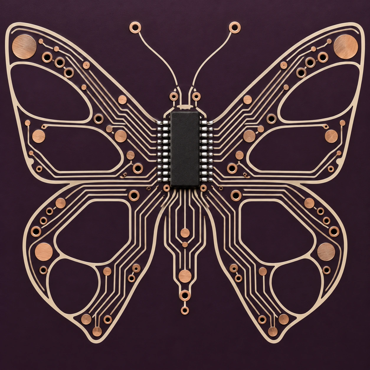
The ginkgo study uses radiating tracks to reinterpret veins, keeping a recognisable leaf outline and a quiet surrounding field. The city study turns routing into streets and component packages into buildings. The moth study tests bilateral balance against the small variations of an intricate network. All three retain the board’s recurring units and manufactured surface. Without those constraints, they would become generic technological decoration rather than specific transformations of a PCB.
Making the work and recognising its limits
For an illustration workflow, sketch the large silhouette first, place component-like masses second and route the decorative paths last. Keep line groups separate while adjusting the design. If you use generative imagery, ask for visible pads, vias, material differences and a restrained palette; then inspect whether the details remain coherent. Look for fused pins, accidental track intersections, floating parts, inconsistent scale and meaningless lettering. A beautiful overall impression can hide many local errors.
The visual language works well for technology editorial art, educational covers, speculative landscapes and metaphors of connection. It becomes a cliché when neon glow replaces structure or when every subject is merely covered with random circuitry. When actual electronics must work, move to an appropriate engineering workflow, with a schematic, real footprints, routing constraints and verification. Artistic plausibility and electrical correctness are different tests. The practical composition advice in this article is AOI interpretation grounded in the vocabulary of board design.
Pocket-sized facts
Printed Circuit Board is classified here as a technical visual reference, not a historical art movement.
PCB layout tools distinguish copper, solder mask and silkscreen layers.
Tracks, pads and vias have different roles; an AI-generated illustration is not a verified fabrication design.
Examples worth exploring
The AOI ginkgo, city and moth studies translate routing and component rhythms into three different subjects.
A small poetic detour
Original words from the AOI studio.
Poetry
Ode to the Unlit Board
No city wakes inside you.
No river knows these turns.
Yet every copper passage
keeps a trace of what it learns.
Small islands wait in order;
the dark between them stays.
A thousand careful distances
make room for different ways.
Tonight you carry nothing
but a leaf imagined whole:
its veins arranged in metal,
its silence left in gold.
The prompt workshop
Original creative exercises. These prompts create new illustrations, not documentary evidence.
Start simple: a routed leaf
Create a top-down PCB-inspired artwork of one ginkgo leaf made of radiating copper tracks and circular vias on matte midnight-blue soldermask. Keep track widths consistent and preserve dark gaps between routes. Leave broad negative space around the leaf. Use subtle metallic highlights, no lettering or neon glow. Artistic interpretation, not a functional circuit.
Check that the leaf silhouette survives when the small details are hidden.
Build a miniature electronic city
Create an isometric imaginary city from black chip packages, small ceramic components and silver pins on a deep green board. Route copper streets with disciplined bends toward one large chip plaza. Vary the density between the centre and the perimeter. Warm low light reveals the manufactured relief. No logos or invented labels.
Keep the scale of pins and packages consistent; the architecture is a visual metaphor.
Experiment: a circuit moth
Design a symmetrical moth using copper pads, branched tracks and cream silkscreen contours on matte aubergine soldermask. Give it a black central chip body and broad quiet cells within the wings. Use fine silver joints and restrained studio reflections. No lettering, no neon, no claim of working electronics.
Preserve bilateral structure while varying the track groups enough to avoid mechanical duplication.
A smile from the studio
Jokes
The circuit-board artist requested more negative space. The engineer asked whether it had passed the clearance check.